BGI - Buffered general input
Below is the detailed schematic of the buffered digital inputs.
Schematic:
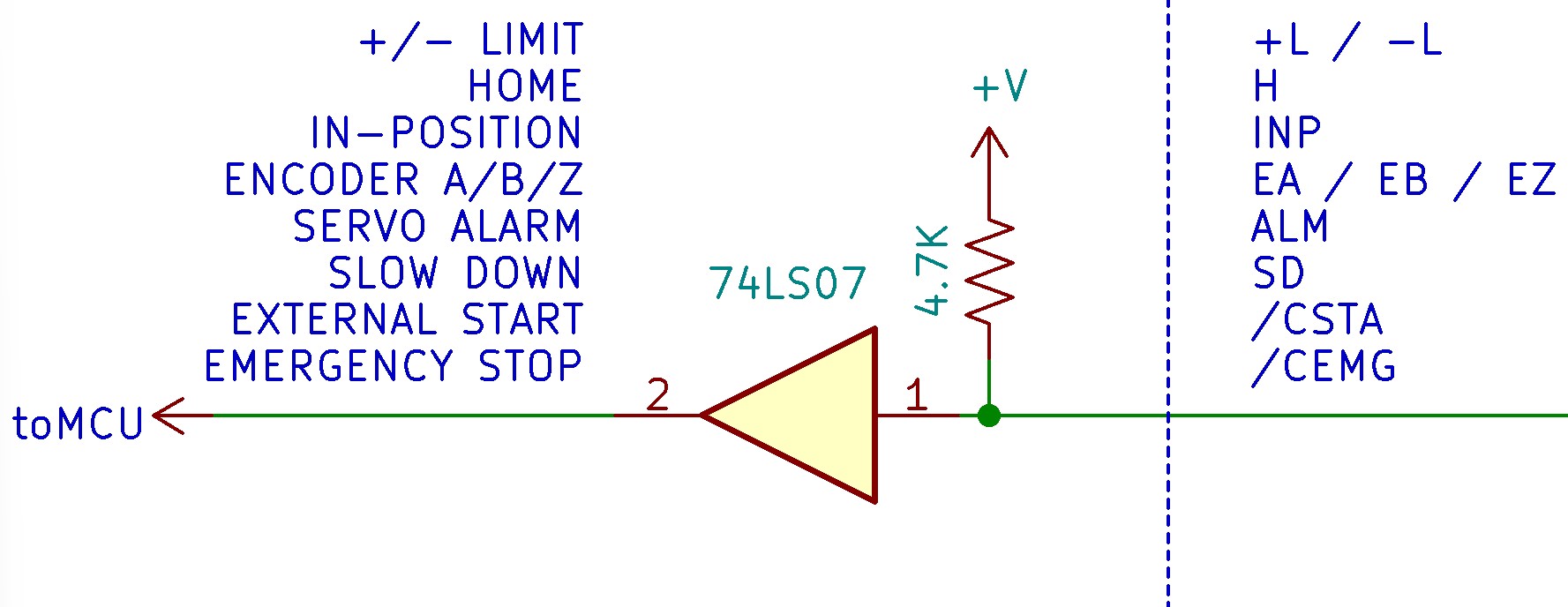
Notes:
The buffered digital inputs are designed to work with open collector (sinking) or TTL logic outputs. When connecting a TTL output, ensure the logic voltage is 5V.
When a digital input is pulled to ground, current will flow from the internal power supply to ground.
To deactivate the input, a digital input should be left unconnected or switched back to the logic supply. This will stop current from flowing.
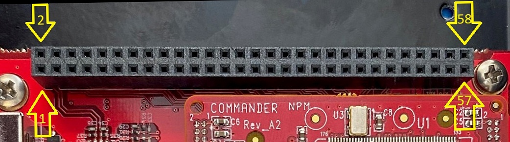
Applies to:
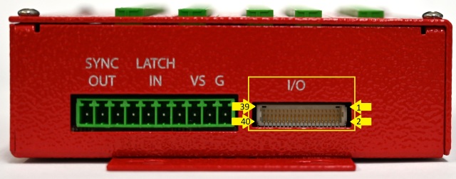
40-PIN DIO connector (I/O Expansion Connector) Pins 2, 29-32, 39
CMD-4EX-SA J7 Pins 5-8, 10-13, 17-20, 22-25, 29-32, 34-37, 41-44, 46-49